In the past year (2022) we gave a talk about this topic in hardwaer.io NL22 but unfortunately the recorded talk faced a technical issues with mic.
Recorded talk:
Also, we got couple of questions and we are sorry for being late but we decided to write a blog to explain the talk in more details… and since then we were busy to do other stuff 😐
Slides URL:
(https://hardwear.io/netherlands-2022/presentation/bypass-NXP-LPC-family-debug-check.pdf)
———
This blog post is structured into the following sections so you can easily navigate!
- LPC introduction
- Dumping LPC bootROM
- bootROM reversing
- CRP History
- The setup
- Power analysis
- The attack
- Effected LPC series
- Conclusion
———
LPC Introduction
NXP LPC family of microcontrollers (LPC 811, LPC 1114, LPC 1343, LPC 1751, LPC 2101, LPC 2148, …) implement a specific mechanism to disable the debug port for security and production purposes. By configuring the Code Read Protection value (CRP) in flash memory, the debug interface will be disabled.
CRP is the convention name in NXP other vendors have there own conventions name such as RDP/security bit…
LPC have 3 levels of Read Protection (CRP1/2/and 3) all of them will disable the JTAG, Each level has a dedicated value. The main difference between between them is related to the ISP commands restriction (ISP: it’s a serial protocol to access memory to operations such as (write/read/erase/…))
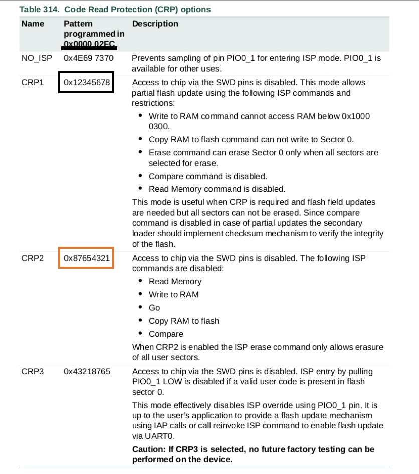
So the user can configure CRP by writing the appropriate CRP value into a specific address in internal flash, and it will trigger the CRP to disable JTAG. For LPC13xx series the address is 0x0000 02FC.
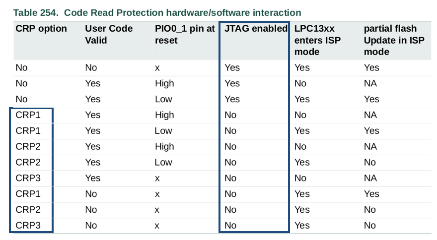
And from this table it’s clear that whenever the CRP is set it will disable JTAG access.
Our objective here is to understand how exactly LPC locking mechanism works and bypass the mechanism of disabling the debug interface by applying voltage fault injection, and to build a reliable attack that can be performed on different versions of the LPC family.
The following diagram shows the memory map of LPC13xx series, and there are 3 interesting areas to us:
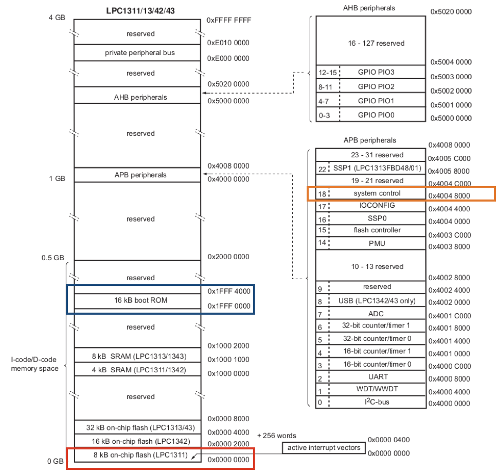
- The RED rectangle is the place where the 0x2FC exist (CRP value)
- The BLUE rectangle is the bootloader which will be dumped
- The ORANGE rectangle is interesting not fully documented address, and is used in disable JTAG (After we reverse engineered the LPC bootROM)
For the LPC boot process the following diagram shows the state where the CRP will be checked
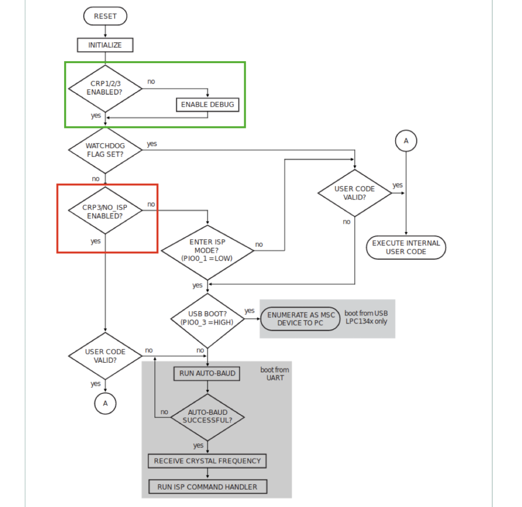
- The GREEN area which will be targeted it’s simply read the content of 0x2FC from internal flash and compare it with any CRP value, in case of matching it will disable JTAG in other cases it will enable it.
- The RED area is where the ISP command restrictions are happened and where the Crhis and others did there work, good to note in this piece of code it will read the 0x2fc content again from internal flash to do the restrictions on ISP commands.
In a Recon Brussels 2017 talk [NXP LPC1343 bootloader bypass], Chris Gerlinsky was able to bypass the bootloader security feature of NXP LPC1343 read and write from flash memory using voltage fault injection.
Enough for introduction let’s go to interesting parts
Dumping LPC bootROM
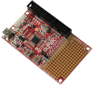
We got open sample of LPC1343 dev board from Olimex as shown in the next picture:
And we have connected to JTAG using JLINK, after establish the debug session we execute the following JLINK command:
 “SaveBin  	SaveBin <filename>, <addr>, <NumBytes> 			Save target memory range into binary file.”

> SaveBin dumpedBootROM.bin 0x1FFF0000 0x4000
bootROM reversing
After we dumped the BootROM we load it to Ghidra and using the SVD LOADER from leveldown security to map the LPC memory map to Ghidra
The main steps that done by this part of the bootROM are:
- At the beginning it will prepare the needed registers and CRP values as follow:
- R3 contain the address of CRP content (0x000002fc in this case)
- R5 contain the CRP3 value
- R6 contain the CRP1 value
- Then Load the content of 0x2fc to R4 register
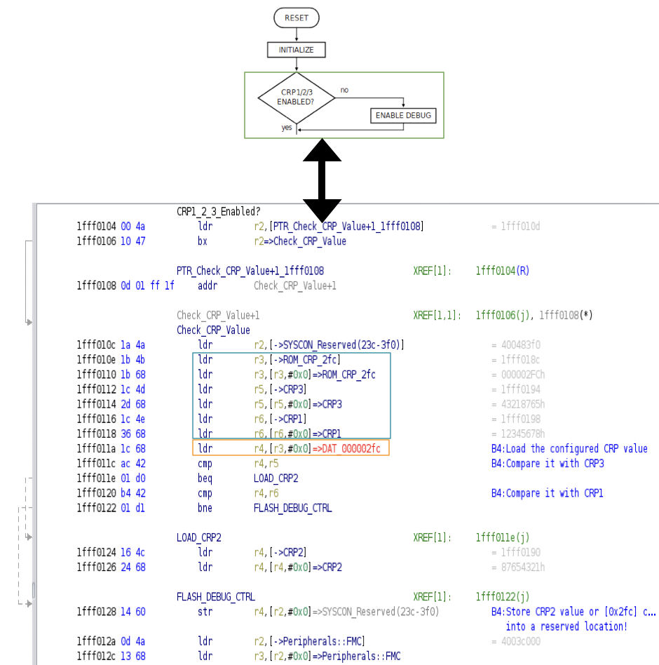
We have 3 main scenarios of execution based on the 0x2FC content
- In case the content of 0x2fc = CRP3, after comparison it will branch to LOAD_CRP2 label to load the CRP2 to r4 register (as shown in small red arrow)
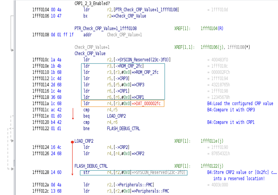
then it will be stored to the SYSCON register to disable JTAG (undocumented), So R4 will contain the CRP2 value to disable JTAG (*R4=0x87654321=CRP2)
- In case content of 0x2fc = CRP1, it will execute all instructions, in the middle as shown in black arrow and It will load the CRP2 value to r4 register then it will be stored to SYSCON register to disable JTAG
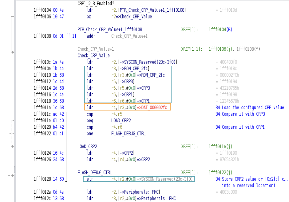
So, again the CRP2 value is used here to disable JTAG.
- In other cases including CRP2 value, it will follow the BLUE arrow and it will branch before Loading the CRP2 value and store whatever the content of R4 to SYSCON register (in case the content is equal to CRP2 value → it will disable JTAG) in other cases it will enable it
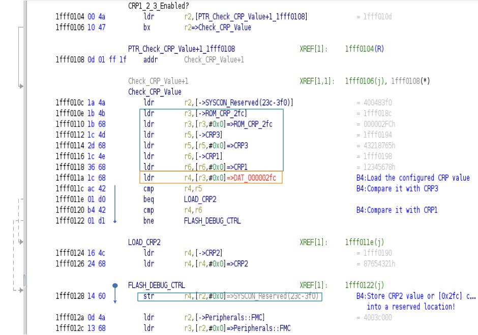
We can notice there is a magic value to disable JTAG which is CRP2 value for all other CRPs!
———
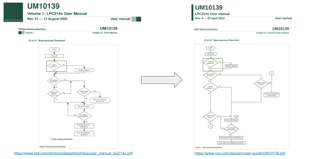
Philips —> NXP
Before 2006 LPC MCU was part of Philips. At Philips time they develop the LPC214x MCU which had a CRP mechanism, So we search for documents from Philips and NXP for the same MCU to compare the boot process and CRP mechanisms
And we found interesting thing…
Here is the boot process for both of them and we can see the NXP introduced CRPs levels!
And here we compare the CRP mechanisms how did they disable JTAG… And from CRP section it seems the MAGIC value used is the same as CRP2!
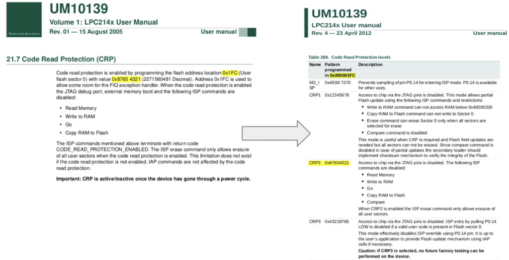
*The value that disables JTAG: 0x8765 4321=CRP2
Bootloader Vulnerability
MCUs will usually startup by initialization the needed components then it will load a configuration from non-volatile memory and finally it will execute the locking mechanism… (chip dependent)
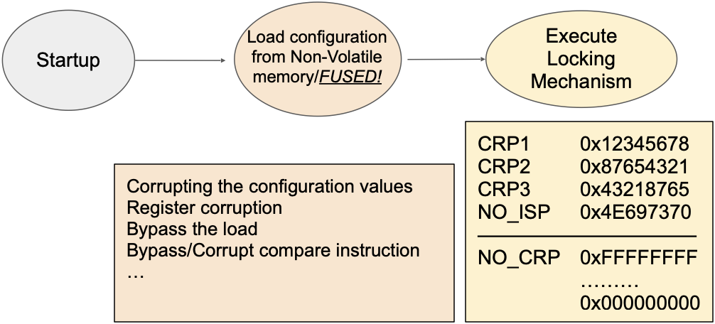
- Most of LPC have a well known design flow regarding the CRP configuration. It’s a 32 bit register where only 3 values have been used to disable the JTAG while the rest will enable it!
———
The setup
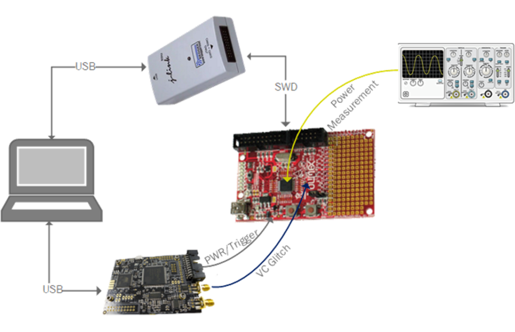
The setup diagram is straightforward.
-The PC is connected to both debug probe [to check the SWD connection] and the Chipwhisperer-Lite [to power the Chipwhisperer and execute code].
*Chipwhisperer-Lite device is incredible device helps you with side-channel power analysis and glitching attacks.
-The debug probe is connected to the Serial Wire Debug (SWD) external connection plug in the LPC target.
-The Chipwhisperer and the oscilloscope connected to the LPC device [more details below].
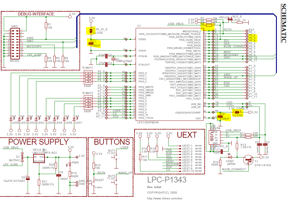
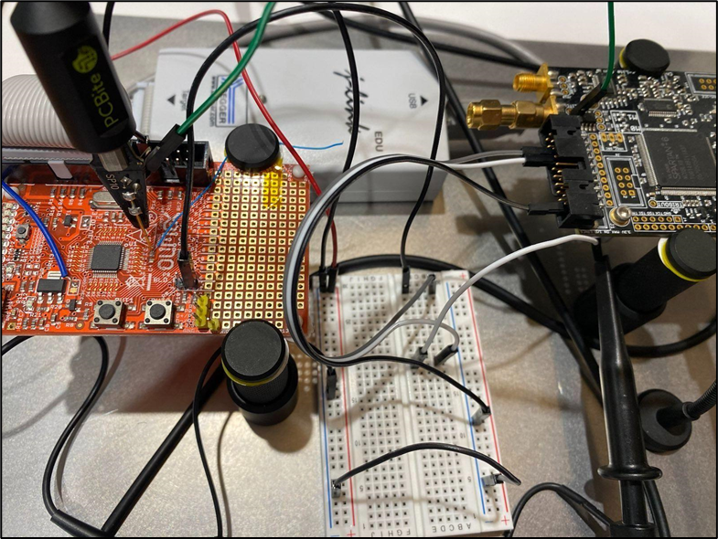
To be able to perform the attack on the LPC target, the bypass capacitors must be removed to make the device glitch easily. Bypass capacitors will filter the voltage fault injection. Therefore, after examining the schematic we removed capacitors C1 and C4 [as shown above]. The C4 capacitor pad is then connected with the voltage glitcher in Chipwhisperer [glitch_out]. In another setup we also used the PCBbite where the glitch will come through (and called it the poison needle as shown below). PCBbite is from Sensepeek company and helped us to solder less!
Supplying the power is also from the Chipwhisperer, where it can control the target by powering it ON and OFF before the glitch and after a failed glitch. Finally, cutting the 3V3_CORE jumper and then connecting it with 1K-Ohm (for better traces) resistor then to the Oscilloscope. The oscilloscope trigger connected to the Chipwhisperer pin that handles turning ON/OFF the LPC target.
———
Power analysis
Voltage fault injection is highly depend on power analysis. In our attack we examined the traces when the CRP value is set and when they are erased, this step will allow us a candidate range where we may perform the glitch.
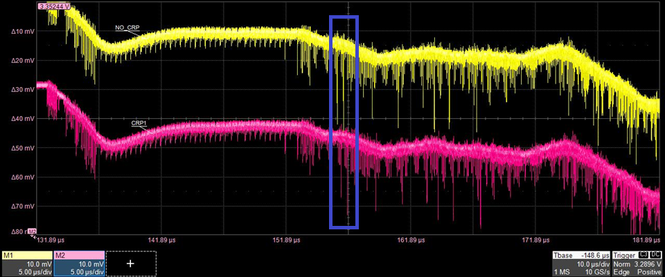
Shown above we captured 2 power traces from LPC1343 the yellow trace when NO_CRP is configured and the pink when we configure it to CRP1. The traces seems similar, except when we looked at the blue rectangle, we observed a latency in pink trace, due to the CRP1 execute more instruction than NO_CRP as explained in the bootROM reversing. We found the sweet spot to be targeted which is after 150us.
———
The attack
We setup the Chipwhisperer-Lite with these parameters to perform the voltage glitch
import subprocess
import chipwhisperer as cw
scope = cw.scope()
def setup_scope():
    scope.clock.clkgen_freq = 100E6 #The clock of CHPW will be 100MHz
    scope.clock.adc_src = "clkgen_x1"
    scope.clock.freq_ctr_src = "clkgen"
    scope.adc.basic_mode = "rising_edge"

def setup_glitch():
    scope.glitch.clk_src = "clkgen" # set glitch input clock
    scope.glitch.output = "enable_only"
    scope.trigger.triggers = "tio3" # The same pin that turns ON/OFF the LPC
    scope.glitch.trigger_src = "ext_single"
    scope.io.glitch_hp = True
    scope.io.glitch_lp = True
    scope.glitch.resetDcms()
for more information about the Chipwhisperer-Lite API
Also we write a function to check on the SWD of the LPC device
def check_swd():
    openocd_command  = "sudo openocd -f /usr/local/share/openocd/scripts/interface/jlink.cfg -c 'transport select swd' -f /usr/local/share/openocd/scripts/target/lpc13xx.cfg -c 'init;exit'"
    check_openocd = subprocess.Popen(openocd_command, shell=True, stdout=subprocess.PIPE,
            stderr=subprocess.PIPE, universal_newlines=True)
    openocd_output = check_openocd.communicate()
    rc = check_openocd.wait()
    print("Return code :", rc)
    print("================================================================")
    print(openocd_output[1])
    print("================================================================")
    if("Error: Error connecting DP: cannot read IDR" in openocd_output[1]):
        print('\n')
        print("###Locked###")
        return 0
    elif("Info : lpc13xx.cpu: hardware has 6 breakpoints, 4 watchpoints" in openocd_output[1] or rc == 0):
        print('\n')
        print("****** UNLOCKED ******")
        return 1
After writing the main functions we defined our glitch parameters, where the offset is around 150us and the repeat from (1 to 16). For more information about the Chipwhisperer-Lite Offset and Repeat
So now we have the range to apply the glitch, the setup was ready, we wrote the code and start glitching. Our trigger first was based on the reset pin, so we were resetting the device wait until the offset then glitch and so on. However, WITH NO LUCK Then we changed the setup, and based the trigger on (power ON/OFF cycle), so we power on the device wait until the range glitch, then power off and so on. After a while we successfully were able to re-enable the debug interface.
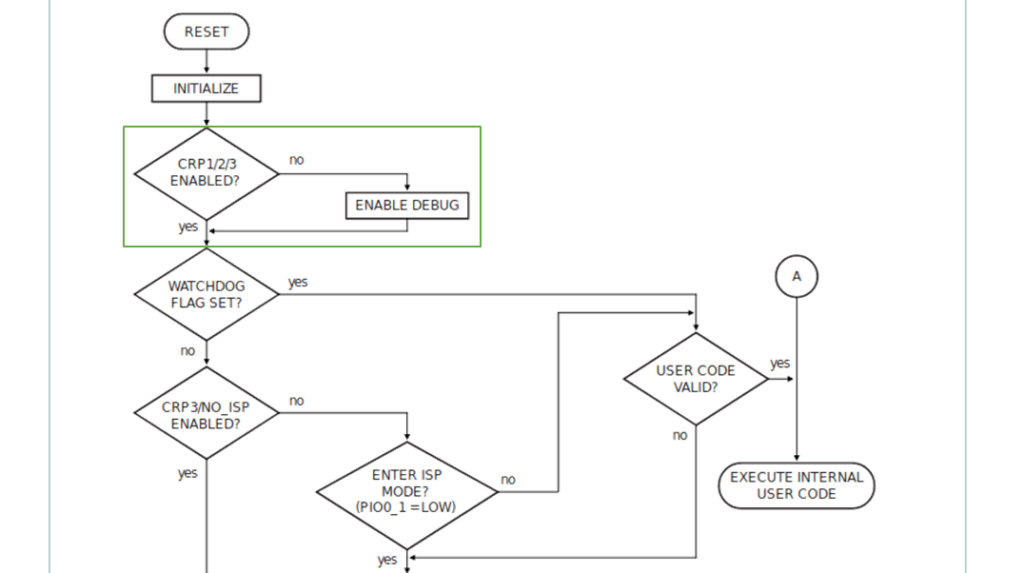
The boot process on RESET was misleading, because it shows (in the green rectangle above) that after each reset it will check the debug. Therefore, our first setup was based on this diagram.
However, when we changed our setup to be based on Power on/off cycle the glitch succeeded and able to unlock the debug interface.
———
Effected LPC series
Based on user manuals we’ve looked at all LPC MCUs and the following list sharing the same CRP mechanism and Boot process diagram, so we assume it might be having the same vulnerability
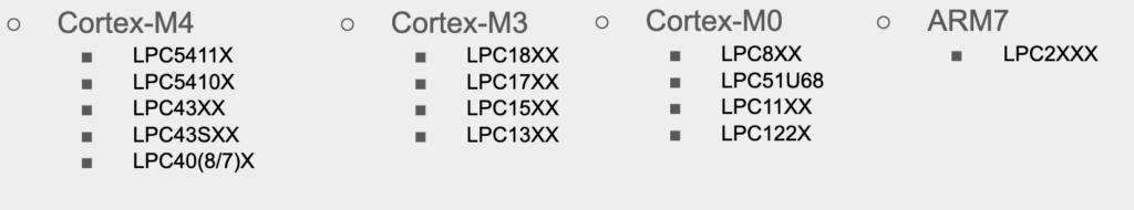
The newer series introduced different locking mechanisms and we didn’t investigated yet:
- ECRP stands for Enhanced CRP which is used in this LPC546 MCUs, based on user manual they have different approach on how JTAG can be enabled by setting a specific bits
- LPC540xx MCU used something called “OTP banks” we have not investigated, but we noticed the bits used for enabling JTAG is 00
- LPC55xx is cortex-M33 which used ARM trustzone, and we didn’t investigated either
———
Conclusion
- We reverse engineered the BootROM and took power consumption traces, and with comparing we found out the range were we should apply our glitch.
- We applied the glitch based on reset trigger with no luck.
- Changed the setup to based our trigger on the power cycle.
- Then we were able to successfully re-enable the debug interface and have full control of the microcontroller.
- Another thing to mention is the CRP locking mechanisms exist since Philips time
- We also contacted NXP to disclose. They were professionals and fast, thanked us for highlighting the misleading step on the boot process diagram.
